
01. Introduction to CC1310
1. feature
The CC1310 is an important component of TI's family of sub-1GHz devices in high-efficiency/ultra-low-power wireless MCUs. Very low active RF and MCU currents and low power mode current consumption ensure battery life and allow for the use of small coin cells in energy harvesting applications.
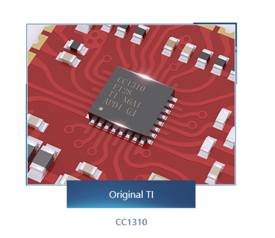
The CC1310 device combines a flexible ultra-low-power RF transceiver with a powerful 48MHz Cortex-M3 microcontroller in a platform that supports multiple physical layers and RF standards. The dedicated wireless controller (Cortex-M0) handles low-level RF protocol commands stored in ROM or RAM to maintain low power consumption and flexibility. The CC1310 device does not achieve low power at the expense of RF performance; the CC1310 device offers excellent sensitivity and stability (selectivity and blocking) performance. The CC1310 device is a highly integrated, true monolithic solution that integrates a complete RF system with an on-chip DC-DC converter. The CC1310 power and clock management and wireless systems require specific configurations and are handled by software to function properly. This goal can be implemented in TI RTOS, so it is recommended that this software framework be applied to all application development processes for devices.
2. Application
The CC1310 device can be used in various frequency bands such as 433M868M915M. It can also be used in automatic meter reading, home and building automation, wireless alarm and security systems, industrial monitoring and security control, wireless medical, active RFID and other fields.
3. Package description
The CC1310 is available in three packages, 4mm x 4mm RSM VQFN48 (10 GPIO), 5mm x 5mm RHB VQFN48 (15 GPIO), 7mm x 7mm RGZ VQFN48 (30 GPIO). As shown below:

No matter which packaged chip is referenced on the 433M wireless module, the RGZ package 7X7 is used as an example to introduce the circuit design. The circuit is divided into two parts: the design of the schematic and the design of the PCB.
02. Schematic Design
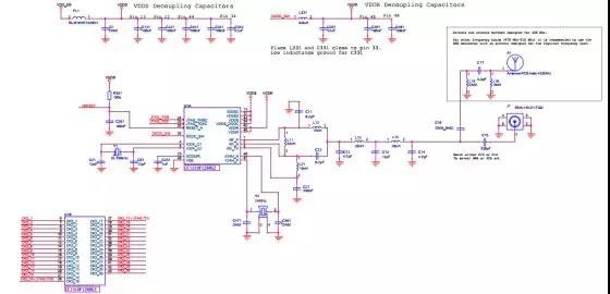
The overall frame: power circuit, reset and crystal circuit, RF circuit and external pin circuit are composed of four parts.
1.Power Circuit
The power circuit is mainly divided into two parts: the power supply circuit and the power switch circuit inside the device. For the power supply circuit, the main purpose is to filter the processing to reduce the ripple to ensure the power supply is stable.

This part of the circuit is a power supply circuit. First, the power supply is connected to FL1 (fuse) as soon as it comes in, which acts as an overload protection. Then, to supply power to each power pin of the chip, a filter capacitor is needed to achieve a power supply and a filter capacitor to ensure the stability of the power supply.
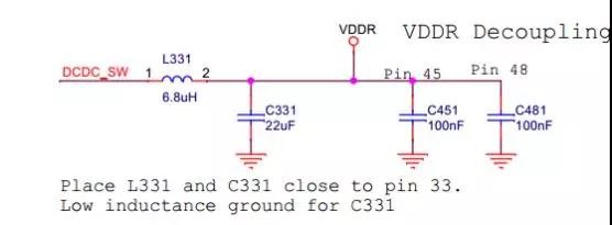
This part of the circuit is the power switch circuit inside the device. When VDDR (ie DCDC_SW terminal) is equal to 1.95V and VDDS minimum voltage is 2.1V, the device can output about 14dBm in the 433M frequency band. In the PCB design, pay attention to L331 and C331 close to the 33rd pin DCDC_SW of the device, put the corresponding filter capacitor to the corresponding power supply pin (should be as close as possible to the power supply pin), and filter it.
2.Reset and Crystal Oscillator Circuit

The reset circuit is an ordinary RC circuit. The device has a high-speed clock 24M crystal oscillator circuit and a low-speed clock 32.768K crystal oscillator circuit. Generally, a 24M crystal oscillator circuit is used. Due to the matching capacitance of the 24M crystal oscillator inside the chip, the two matching capacitors C471 and C461 are generally reserved. The 32.768K crystal oscillator circuit is used as a reserve (usually not used), plus two 15pF matching capacitors.
2. RF Circuit
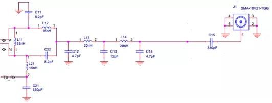
The RF circuit is mainly composed of a balun and a fifth-order filter. C15 is a DC blocking capacitor with a size of 330pF. Pay particular attention to the fact that C13 and C14 cannot be excessively increased during RF debugging, otherwise power will drop.
4.Peripheral Circuit
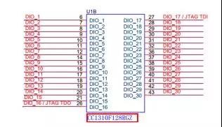
03. PCB Design
1.Overall layout reference
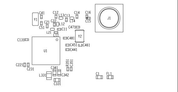
The layout is mainly the layout of the RF circuit, and the layout between the inductor and the inductor is avoided to avoid mutual inductance, preferably vertical. There is also the layout of the power supply circuit. As long as the power supply has a capacitance to the ground, it is better to add at least one ground via.
2.Overall Wiring Reference
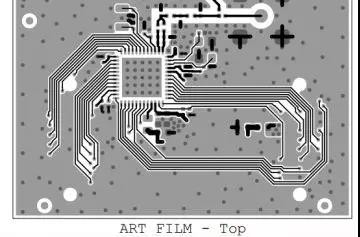
The layout directly affects the wiring. Note: Do not have a loop on the power wiring to avoid forming a power loop. RF wiring should be as short as possible to reduce the loss of RF signals.