Introduction
The nRF52810 SoC uses the same 100dBmlink budget 2.4GHz multi-protocol radio as the nRF52832 SoC and is equippedwith a 64MHzh 32-bit ARM Cortex-M4 MCU to meet demanding performance requirements;it uses the same hardware and software as other nRF52 series SoCs.Architecture, which means that migration between nRF52 series isstraightforward. At the same time, although the nRF52810 is a basic Bluetooth 5SoC, there are still many common peripherals available - compared to thenRF52832's 512kB flash and 64kB RAM, it integrates 196kB flash and 24kB RAM,enough to run typical high throughput, low-Cost application code and supportfor device firmware update (OTA-DFU) for target applications via over-the-airtechnology. In addition, the nRF52810 is compatible with the nRF52 DevelopmentKit (DK), and the application code compiled for the device is portable to allSoCs in the nRF52 family. Users can use the parallel multi-role S132 protocol stacksupporting 20 links and the nRF5 SDK when developing application software.
RF chip: NordicnRF52810
Carrier frequency: 2.4GHz
Product size: 17.5*28.7mm
Power: 2.5mW
Communication distance: 110 meters
Small size, built-in ARM microcontroller,users need to conduct a secondary development.
ARM® Cortex ®-M4 32-bit processor, 64 MHz
2.4GHz frequency band
Flexible power management
1.7 V-3.6 V supply voltage range
Fully automatic LDO and DC/DC regulatorsystem
Fast wake-up using 64 MHz internal oscillator
0.3 µA at 3 Vin System mode, no RAM retention
0.5 µA at 3 V in System mode with full 24 kB RAMretention
192 kB flash and 24kb RAM
Support for concurrent multi-protocol
12-bit, 200 ksps ADC - 8 configurable channels with programmable gain
Temperature Sensor
Up to 32 general purpose I/O pins
4-channel pulse width modulator (PWM) unitwith EasyDMA
Digital Microphone Interface (PDM) • 3x 32-bittimer using counter mode
SPI master/slave with EasyDMA•I2C compatible 2 -wire master/slave
UART (CTS / RTS) Easy DMA • ProgrammablePeripheral Interconnect (PPI)
Cross decoder (QDEC) • AES HW encryption for easydirect memory access
2x real time counter (RTC)
Package size
• QFN48, 6×6mm
• QFN32, 5×5mm
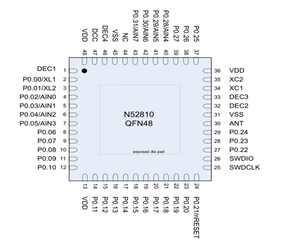
Pindefinition
The design ofthe two packages is the same, here is the example of QFN48

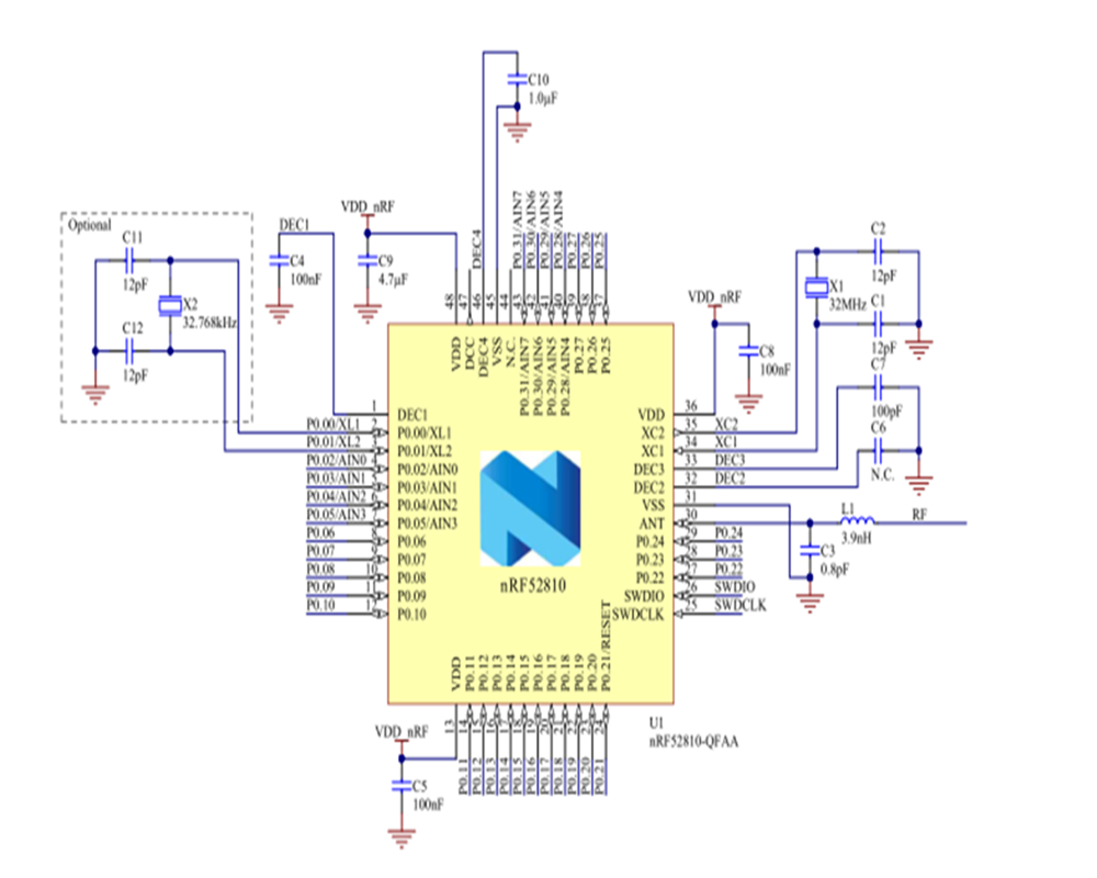
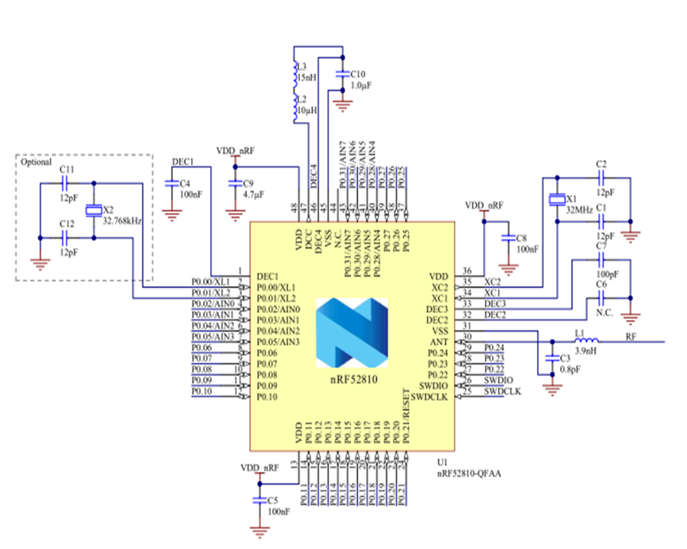
Designschematic diagram

Figure 2 Internal LDO settings

Figure 3 DC / DC settings