In our circuit design, communication level conversion problems are often encountered, and it is necessary to judge the necessity of level conversion before applying level shifting measures.
If you are using a 3.3V device as the output and a 5V device as the receiver, then this low level output will not damage the device, and most 3.3V devices can also meet the high power of 5V devices when the output is high. Flat input standard, you don't need level shifting at this time. The only caveat is that if the external 5V device needs to draw current from a 3.3V device, you need to consult the maximum value of the current drawn on the interface in the data sheet. Add buffers (such as the 74HC245) if needed.
If, in turn, you want to use a 5V output device to drive a 3.3V peripheral, you need to consider the need for a level shifting device. But some 3.3V chips have been designed to withstand 5V input. Such a chip can be directly driven by a 5V master directly. The most classic example is the 74LVC series chip.
The CMOS device's criteria for high and low levels is not a specific value, but is based on the percentage of the supply voltage. In general, the high-level standard of CMOS devices should be greater than 0.7 times the supply voltage (that is, the high-level standard will be 3.5V when powered by 5V), which will result in a high level of 3.3V. Unable to trigger. But this is not absolute, some devices can work normally at 3.3V level, even if the nominal normal operating voltage is 5V. For this type of problem, it is best to use a device that is compatible with the 3.3V level standard.
For TTL devices, the standard for determining the high level when operating at 5V is the determined 2V. This is also the reason why the level can be judged normally when using a TTL device in one direction.
Now let's introduce several common communication level conversion schemes.
(1) Transistor + pull-up resistor method
It is a bipolar transistor or MOSFET. The C/D is connected to a positive pull-up resistor. The input level is very flexible and the output level is roughly the positive power level.

Communication Level Conversion Guide
(2) OC/OD device + pull-up resistor method
Using OC or OD gate circuit, the collector or the drain can be pulled up to anew VCC through a resistor, and the base or gate can be connected to anotherVCC, thus achieving 3.3V control of 5V. Flat signal output. Note that thepull-up resistor value needs to be selected here, and the drive capability ofthe MCUIO should also be considered. Most of these circuits use level shiftingcircuits on the output circuits.
(3) 74xHCT series chip boost (3.3V & rarr; 5V)
Any 5V CMOS device with input 5V TTL level compatibility can be used as a 3.3V &rar; 5V level shifter.
—— This is because the level of 3.3V CMOS is justcompatible with the 5V TTL level (coincidence), and the output level of CMOS isalways close to the power level.
Cheap options such as the 74xHCT (HCT/AHCT/VHCT/AHCT1G/VHCT1G/...) series (thatletter T means TTL compatible).
(4) Dedicated level shifting chip
3.3V and 5V are converted using a specific level shifting chip. For example,74LVC4245A and 74ALVC164245 are used in more than two chips. It has 5V VCCA and3.3V VCCB, 2 power pins, so that 5V and 3.3V conversion can be realized, andDIR controls the data direction, which also realizes 3.3V to 5V, and 5V to3.3V. Direction conversion. In addition, the 74LVC4245A can also increase thecurrent drive capability of the MCUIO. I would prefer this chip if I need it inmy design. The 74ALVC164245 is 16Bit and functions similarly to the 74LVC4245A.
(5) Resistance division method
The easiest way to lower the level. The 5V level is divided by 1.6k+3.3kresistor, which is 3.3V.

Communication Level Conversion Guide
(6) Current limiting resistor method
If there are too many resistors on the top, sometimes only one current limitingresistor can be connected in series. Although some chips do not allow the inputlevel to exceed the power supply in principle, it is safe to connect a currentlimiting resistor in series to ensure that the input protection current doesnot exceed the limit (eg 20mA for the 74HC series).
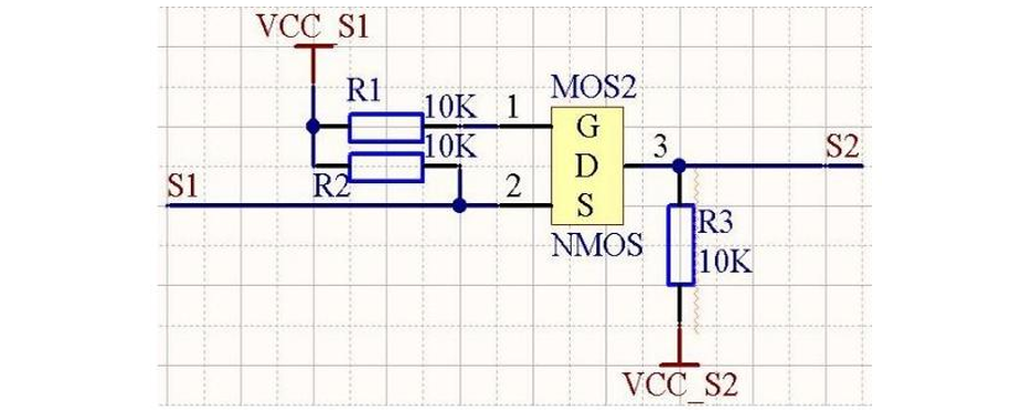
Finally, here is a simple classic circuit that can achieve two levels of mutualconversion.
Communication Level Conversion Guide

In the above figure, S1 and S2 are two signalterminals, and VCC_S1 and VCC_S2 are the high-level voltages of these twosignals. The other restrictions are: 1. VCC_S1<=VCC_S2. 2, the low-levelthreshold of S1 is greater than 0.7V. Left and right (depending on the diodevoltage drop in NMOS). 3, Vgs<=VCC_S1. 4, Vds<=VCC_S2 For the mutualconversion of 3.3V and 5V/12V circuits, the NMOS transistor can select AP2306,the principle is relatively simple.
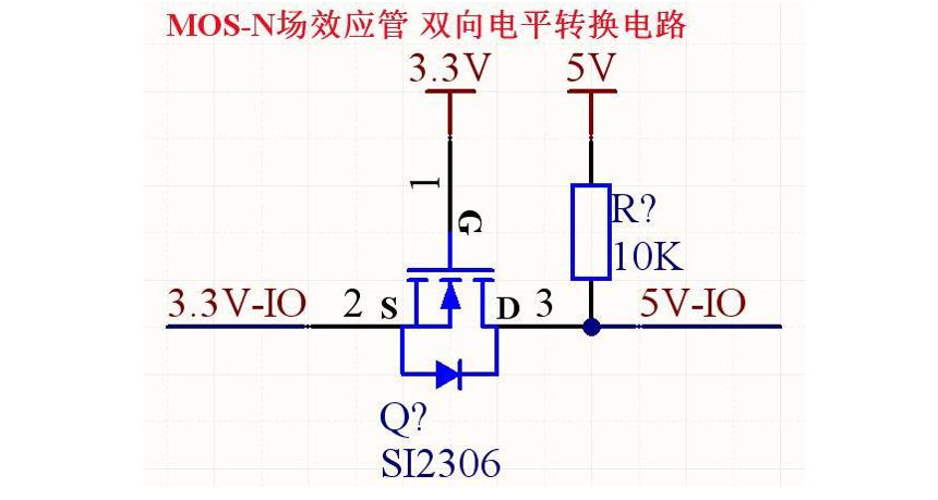
The following figure shows the MOS-N FET bidirectional level conversion circuit- suitable for simple applications of low frequency signal level shifting.
Communication Level Conversion Guide
The circuit shown above, the principle of two-way transmission: For theconvenience of description, 3.3V is defined as A terminal and 5.0V is Bterminal. When the A terminal outputs a low level (0V), the MOS transistor isturned on, the B terminal output is low level (0V), the A terminal output is highlevel (3.3V), the MOS transistor is turned off, and the B terminal output ishigh level (5V). When the A terminal outputs high impedance (OC), the MOStransistor is turned off, the B terminal output is high level (5V), the Bterminal output is low level (0V), and the diode in the MOS transistor isturned on, thereby turning on the MOS transistor, the A terminal The output islow level (0V) B terminal output high level (5V), MOS tube is cut off, Aterminal output is high level (3.3V) B terminal output high resistance (OC),MOS tube is cut off, A terminal output Is the high level (3.3V) advantages: 1,suitable for low-frequency signal level conversion, low price. 2. After theconduction, the voltage drop is smaller than the triode. 3, forward and reversedouble-conducting, equivalent to mechanical switches. 4, voltage type drive, ofcourse, also requires a certain drive current, and some applications may belarger than the triode.